 Quick Summary: The Four PTFE Manufacturing Challenges
Key point: PTFE PCB manufacturing has four specific challenges with no FR4 equivalent: (1) hole wall activation — PTFE is chemically inert, copper will not bond without plasma or sodium naphthalene treatment; (2) drilling — PTFE softens under heat, standard FR4 parameters cause hole wall smearing; (3) lamination — PTFE requires different press profiles, specific bonding films, and a strict 2-cycle maximum; (4) dimensional stability — PTFE has higher CTE than FR4, dimensional management is more critical. Skip any of these and the boards will fail — some immediately, some after thermal cycling in the field.
Challenge 1: Hole Wall Activation
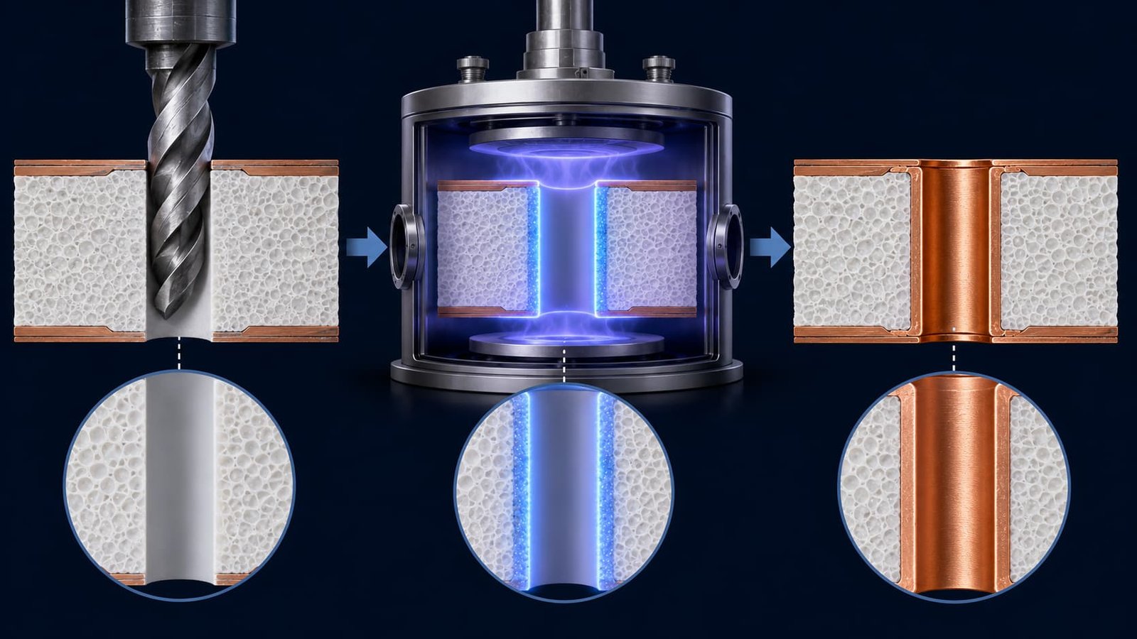
This is the most critical PTFE manufacturing challenge — and the one most often skipped by factories without genuine PTFE capability. PTFE (polytetrafluoroethylene) is one of the most chemically inert materials known. The same property that gives it low dielectric loss also prevents copper from bonding to the PTFE hole wall surface.
During standard PCB manufacturing, electroless copper is deposited on the hole walls to make them conductive before pattern plating. On FR4 and Rogers hydrocarbon materials, the resin surface accepts electroless copper deposition naturally after desmear. On PTFE, the copper deposits as a thin film with essentially no adhesion — the surface is too inert to form a chemical bond.
What Happens Without Activation
- Electroless copper deposits on the PTFE hole wall but has no adhesion
- The board passes all initial electrical tests — continuity looks normal
- After 50–200 thermal cycles, the copper separates from the PTFE hole wall
- The via opens — a complete circuit failure
- This failure is expensive: the board was accepted, assembled, installed, and operated before failing
- In aerospace and defense applications, field failure is catastrophic
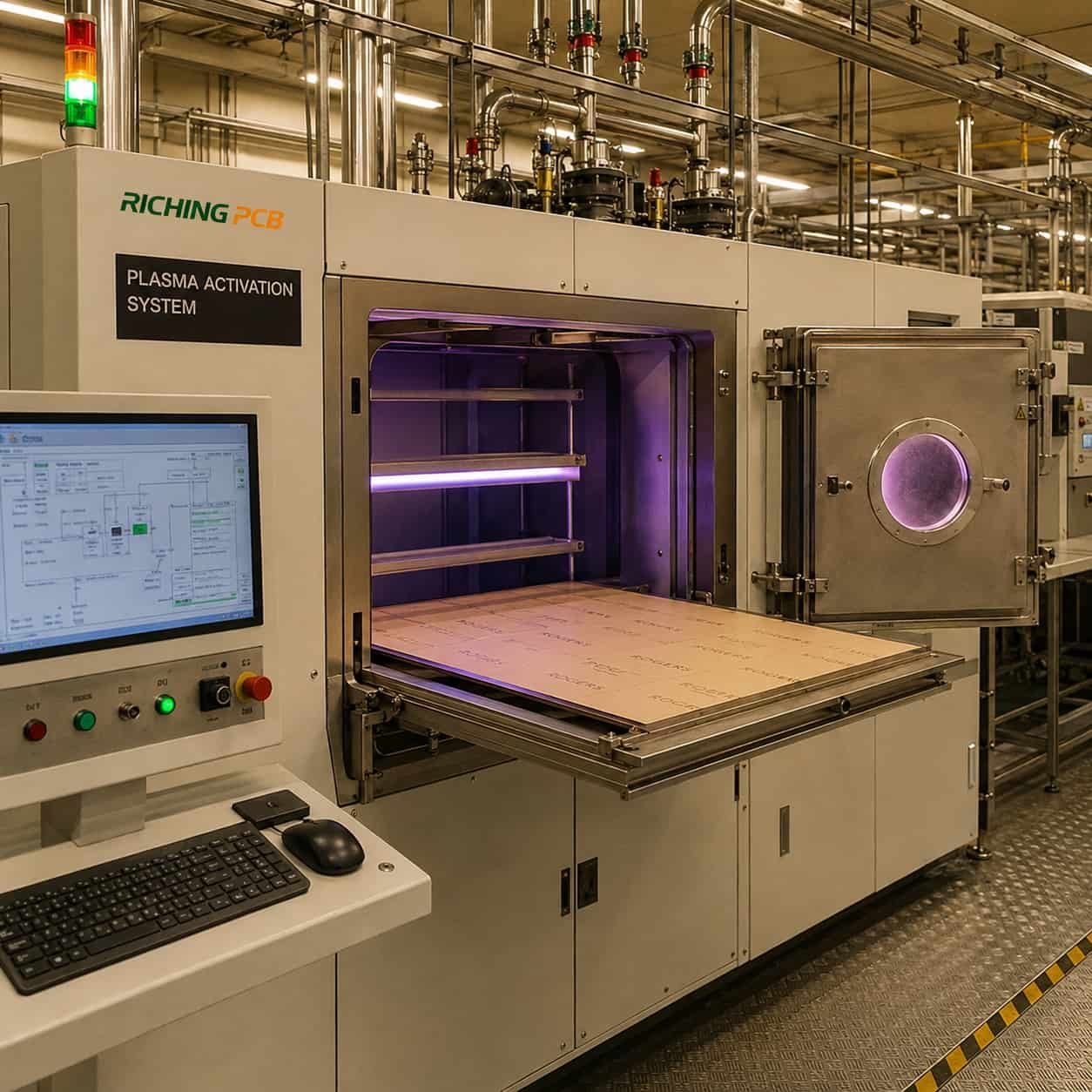
Activation Method 1: Plasma Activation
RF plasma activation uses a plasma chamber to etch the PTFE hole wall surface at the molecular level. The plasma removes fluorine atoms from the PTFE surface, leaving carbon radicals that form polar functional groups. These groups accept electroless copper deposition reliably.
- Equipment: dedicated plasma activation chamber — this is our standard method
- Process: 5–15 minutes exposure depending on board thickness and hole count
- Gas: oxygen or argon/oxygen mixture — creates active plasma that etches PTFE surface
- Result: uniform activation across all hole walls, including small-diameter vias
- Advantage: clean process, no hazardous chemical waste, consistent activation depth
- Verification: pull test on activated sample before production — copper should not peel from hole wall
Activation Method 2: Sodium Naphthalene
Sodium naphthalene (sodium-naphthalenide) dissolved in tetrahydrofuran (THF) etches the PTFE surface chemically, removing fluorine atoms and creating a bondable surface. This method was the standard before plasma systems became widely available.
- Process: immersion in sodium naphthalene solution for controlled time
- Result: dark brown discoloration of the PTFE surface — normal and expected
- Advantage: no capital equipment cost, effective for all PTFE grades
- Disadvantage: THF is a hazardous solvent requiring careful handling and disposal, sodium naphthalene is moisture-sensitive
- Less common in modern factories: plasma has largely replaced sodium naphthalene due to cleaner process
How to Verify a Factory Has Genuine PTFE Activation
Ask this question before placing any PTFE PCB order: ‘What hole wall activation method do you use for Rogers RO3003?’ A factory that processes PTFE regularly answers immediately and specifically — plasma or sodium naphthalene. A factory that does not process PTFE will give a vague answer, say they use ‘standard desmear’, or need to check.
Standard desmear is NOT activation: Permanganate desmear removes resin smear from FR4 and Rogers hydrocarbon hole walls. It does nothing useful for PTFE surfaces. A factory that says ‘we use standard desmear for all materials’ does not have PTFE activation capability — their PTFE boards will have unreliable PTH connections.
Challenge 2: PTFE-Specific Drilling
PTFE is mechanically softer and has different thermal properties than FR4. Standard FR4 drill parameters — spindle speed, feed rate, chip load, entry and exit materials — cause problems when used on PTFE laminates.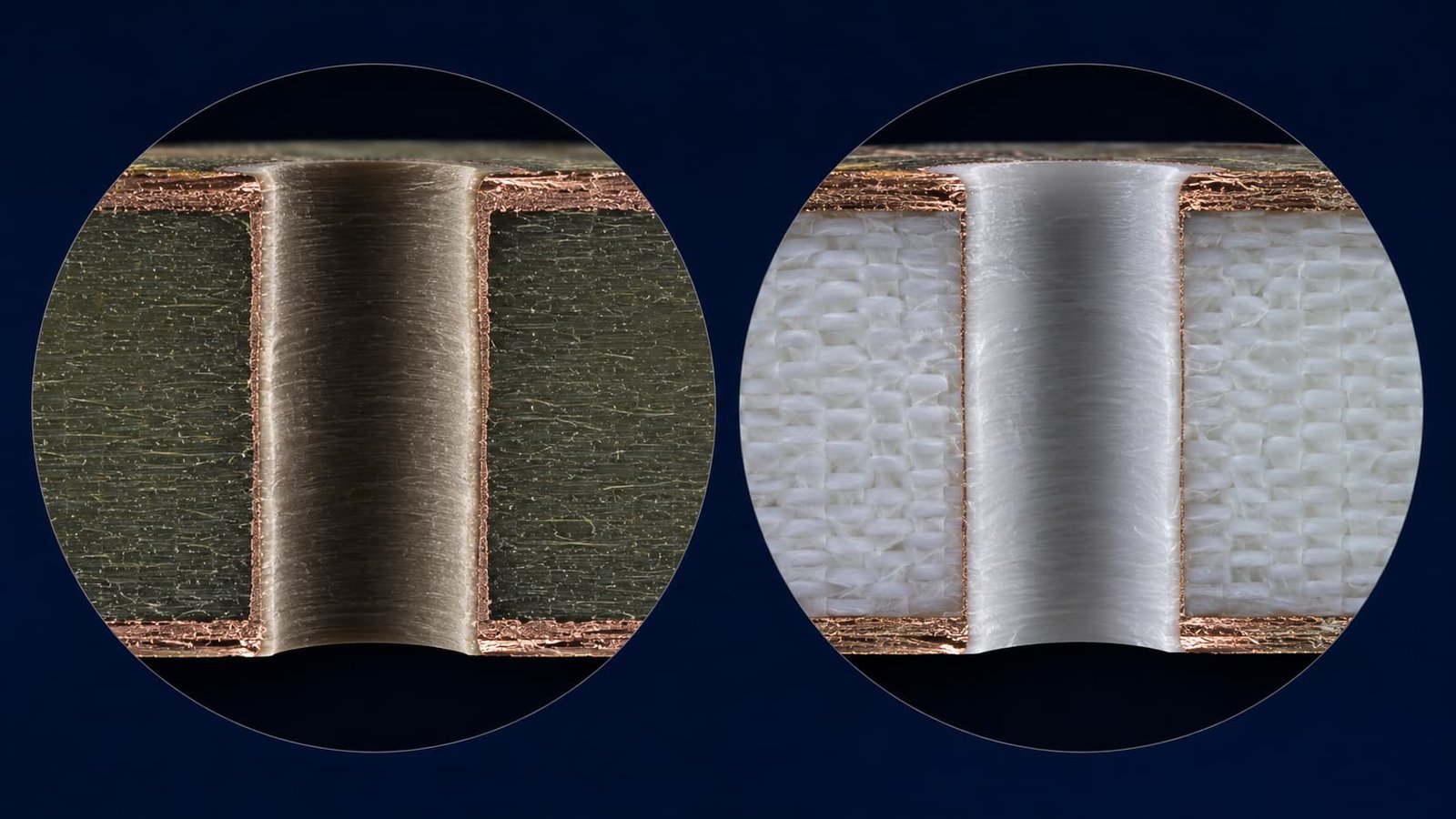
The Problem With Standard FR4 Drill Parameters on PTFE
- High spindle speed generates heat at the drill tip through friction — PTFE softens and smears into the hole wall at elevated temperatures
- Smeared PTFE on the hole wall is even more difficult to activate than clean PTFE — the smear layer must be removed before activation
- High feed rate causes mechanical deformation of the soft PTFE — hole walls become oval or irregular
- Standard entry board materials allow surface burring on PTFE — the soft material tears rather than cuts cleanly at the drill entry
PTFE-Specific Drill Parameters
- Spindle speed: 30–50% lower than FR4 — prevents thermal softening at the drill tip
- Feed rate: 20–40% lower than FR4 — reduces mechanical stress on PTFE
- Chip load: adjusted to prevent PTFE from sticking to drill flutes
- Entry material: PTFE-specific aluminum entry board — prevents surface burring
- Backup material: PTFE-compatible backing board — clean exit hole
- Drill bit replacement: more frequent than FR4 — PTFE work-hardens drill edges faster
- These parameters are confirmed for Rogers RO3003, RT5880, Taconic TLY-5, RF-35, and F4B series at our factory
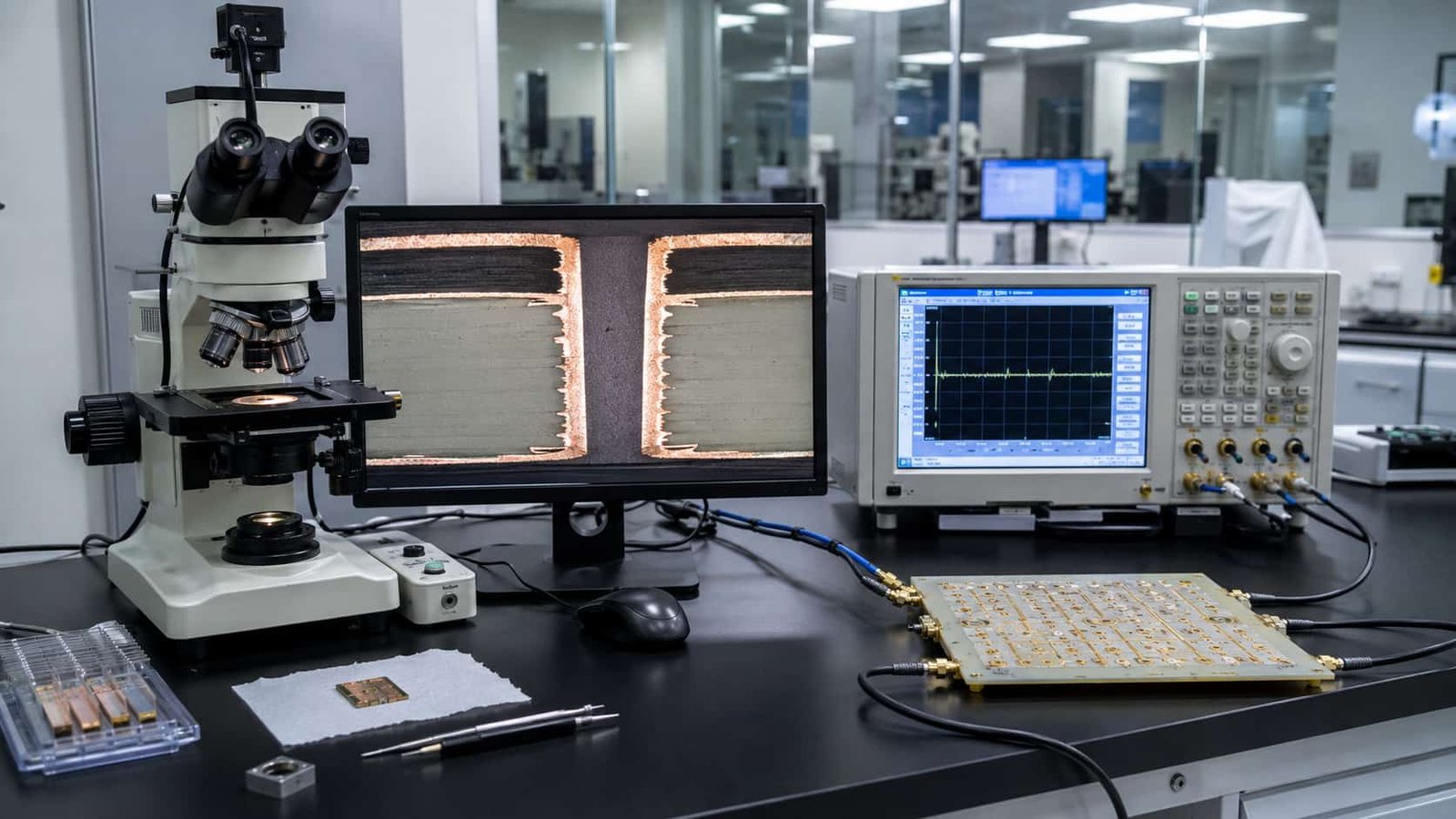
Hole Quality Verification for PTFE
- Hole wall smoothness: inspect with optical microscope or SEM — smear indicates wrong parameters
- Hole roundness: verify with 2D measurement — oval holes indicate feed rate too high
- Entry and exit quality: inspect for burring at hole entry and exit
- For Ka-band designs with 0.127mm substrate: drill quality is critical — thin substrates amplify the consequences of parameter errors
Challenge 3: Lamination
PTFE lamination has three specific requirements that differ from FR4 and Rogers hydrocarbon materials: a different press temperature profile, a different bonding film, and a strict 2-cycle maximum.
PTFE Press Temperature Profile
PTFE softens at different temperatures than FR4 epoxy. The press temperature profile must be carefully controlled to achieve complete bonding without causing PTFE to flow excessively under heat and pressure.
- Temperature: PTFE-specific profile — higher than FR4 in some phases, controlled ramp rate
- Pressure: controlled to prevent PTFE flow — excess pressure at elevated temperature causes PTFE to deform and change dielectric thickness
- Cooling rate: controlled to prevent warpage — PTFE higher CTE than FR4 means faster cooling creates more stress
- Equipment: standard press equipment is adequate — the profile, not the equipment, is PTFE-specific
Bonding Film Selection — Critical for Hybrid Stackups
The bonding film used at Rogers-Rogers and Rogers-FR4 interfaces in hybrid stackups must be matched to the dielectric material. Using the wrong bonding film creates both an electrical problem (impedance discontinuity) and a mechanical problem (unreliable bond).
- Rogers RO3003 and RT5880 hybrids: Rogers 2929 bondply — specifically formulated for PTFE surfaces
- Rogers RO4350B and RO4003C hybrids: Rogers RO4450F bondply — for hydrocarbon ceramic surfaces
- Standard FR4 prepreg: NOT suitable at any Rogers interface — wrong Dk, unreliable adhesion to Rogers surfaces
- Taconic PTFE: tacBOND or Rogers 2929 — confirm with factory
- F4B PTFE: PTFE-compatible bondply — same requirement as Rogers PTFE
Common mistake: Using Rogers RO4450F (designed for RO4350B) at a Rogers RO3003 or RT5880 interface. RO4450F is a hydrocarbon-based bondply that does not bond reliably to PTFE surfaces. The bond may appear acceptable after lamination and fail under thermal cycling or mechanical stress.
Maximum 2 Lamination Cycles
All PTFE-based materials — Rogers RO3003, RT5880, RO3006, RO3010, Taconic TLY-5, RF-35, F4B series — have a maximum lamination cycle limit of 2. A third press cycle degrades PTFE dielectric properties and via reliability. This limit is non-negotiable.
- 1st cycle: base stackup lamination
- 2nd cycle: blind via stage or additional layer addition — at the PTFE limit
- 3rd cycle: NOT permitted for any PTFE material
- Planning required: blind via structure must be planned before selecting PTFE material — 2 blind via stages require 3 cycles, which is impossible with PTFE
- Rogers RO4350B and RO4003C: maximum 3 cycles — more flexible for complex multilayer designs
Challenge 4: Dimensional Stability
PTFE has higher thermal expansion coefficients than FR4 in some dimensions, and different moisture absorption characteristics. These differences must be managed in panel handling, artwork scaling, and hybrid stackup design.
CTE Mismatch in Hybrid Stackups
- Rogers RT5880 x-y CTE: 31 ppm/°C — significantly higher than FR4 (14–17 ppm/°C)
- Rogers RO3003 x-y CTE: 17 ppm/°C — close to FR4, manageable
- For RT5880 + FR4 hybrid on large panels: warpage analysis recommended before production
- For RO3003 + FR4 hybrid: CTE mismatch is smaller — generally manageable without special measures
Moisture and Dimensional Change
- PTFE moisture absorption: 0.02–0.04% — much lower than FR4 (0.10–0.20%)
- Low moisture absorption means minimal Dk change in humid environments — an advantage for RF performance
- But: PTFE must be dried before lamination — any absorbed moisture during storage creates void risk during press
- Storage: PTFE laminates kept in dry conditions — sealed packaging until use
The Most Common PTFE PCB Failure Modes
Failure 1: PTH Open After Thermal Cycling
- Symptom: board passes initial test, fails after 50–500 thermal cycles
- Root cause: no hole wall activation or inadequate activation — copper not bonded to PTFE
- Detection: microsection cross-section shows copper separated from PTFE hole wall
- Prevention: confirm plasma or sodium naphthalene activation before ordering
Failure 2: Impedance Out of Tolerance
- Symptom: TDR measurement shows impedance significantly outside ±10%
- Root cause: wrong Dk used in calculation (nominal vs confirmed lot); wrong bonding film Dk contribution; dielectric thickness variation from press
- Prevention: factory uses confirmed lot Dk from Rogers certificate; correct bondply specified
Failure 3: Delamination in Hybrid Stackup
- Symptom: layers separate at Rogers-FR4 interface, visible as white areas or blistering
- Root cause: wrong bonding film — FR4 prepreg or RO4450F used instead of Rogers 2929
- Prevention: confirm Rogers 2929 bondply in factory inventory before ordering PTFE hybrid
Failure 4: Hole Wall Smear / Irregular Holes
- Symptom: poor plating adhesion in specific via sizes, irregular hole shape on inspection
- Root cause: standard FR4 drill parameters used on PTFE — thermal smearing or mechanical deformation
- Prevention: factory confirms PTFE-specific drill parameters for the material and hole size
Failure 5: Board Warpage
- Symptom: board bows after lamination or during reflow, fails flatness requirement
- Root cause: CTE mismatch in hybrid stackup, incorrect press cooling rate, or 3rd lamination cycle on PTFE
- Prevention: warpage analysis for RT5880 + FR4 hybrid large panels; never exceed 2 press cycles
How Our Factory Addresses Each PTFE Challenge
- Hole wall activation: plasma activation chamber — in-house, standard for all PTFE materials, no exceptions
- Drilling: confirmed PTFE-specific parameters for RO3003, RT5880, Taconic TLY-5, RF-35, CER-10, F4B series
- Bonding film: Rogers 2929 bondply in stock — confirmed before every PTFE hybrid order
- Lamination: maximum 2 cycles strictly enforced — tracked in production order documentation
- Dimensional: PTFE laminates stored in dry conditions, dried before use
- Impedance: confirmed lot Dk from Rogers or Taconic material certificate used in every calculation
- Quality: TDR impedance on every lot, microsection FAI available for IPC Class 3 programs
For full PTFE material properties and applications, see PTFE PCB: Material Properties, Manufacturing Process and Applications. For Rogers RO3003 manufacturing, see Rogers RO3003 PCB: Ka-Band, 77GHz and Defense Applications Guide. For Rogers RT5880, see Rogers RT5880 PCB: EW, SIGINT and W-Band Applications Guide.